Key Features
- Efficient step-down voltage conversion.
- Simulation tools: LTSpice for stability and performance analysis.
- Applicable for embedded systems and power electronics.
Buck Converter Overview
A buck converter is a DC-DC step-down power supply circuit that reduces the input voltage to a lower output voltage. It uses switching regulators to maintain efficiency and consists of key components such as an inductor, capacitor, diode, MOSFET switch, and controller.
Design
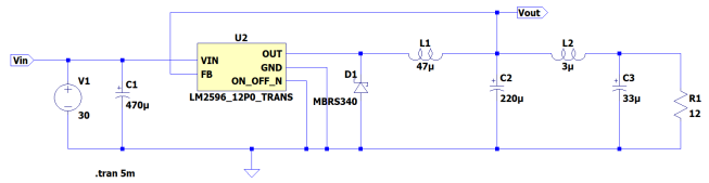
Figure 1: Schematic design interface
Testing and Results
The fabricated PCB was tested using a power supply of 30V input, and the output voltage was measured using a multimeter. The expected output voltage was 12V, but the measured value was 11.84V, leading to a deviation of approximately 1.42%.
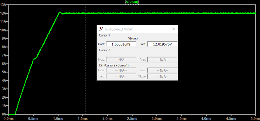
Figure 2: LTSpice simulation result
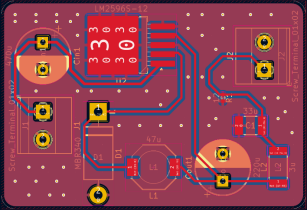
Figure 3: PCB Layout
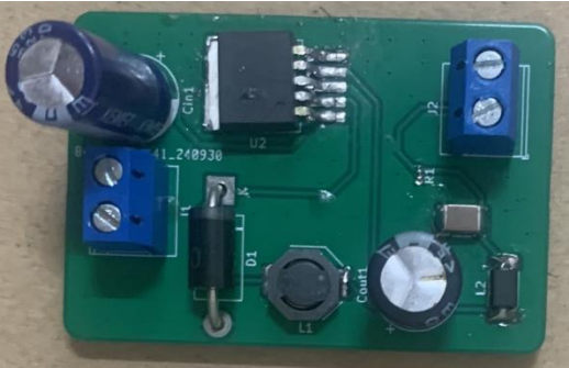
Figure 4: PCB after soldering
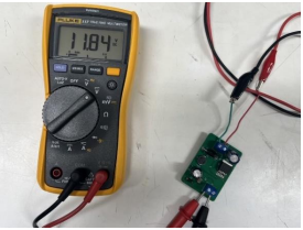
Figure 5: Measured Output Voltage
Challenges and Observations
- Incorrect component footprints caused difficulty in sourcing compatible parts.
- Issues with component polarity required rework.
- Measured output was slightly lower than expected due to component tolerances.
Conclusion
The project successfully demonstrated the design, simulation, and testing of a buck converter. The results were within an acceptable error margin, making the design viable for real-world applications.
← Back to Projects